Two weeks ago we started a blog series about operational amplifiers aka. opamps (or op amps). We showed you what an opamp is, some of the things it can do and the importance of feedback. To ensure that everything was as easy to understand as possible, we looked at the opamp as an ideal component. However, in reality, just like other electrical components, they aren’t really ideal. They all have their limitations and “flaws” which you should be aware of when selecting which opamp to use in your circuit. In this blog post we’re going to take a closer look at the more realistic opamp and discuss some of the properties of opamps which are important to understand.
Disclaimer: This blog post is meant as a brief intro to this topic and not as an academic article. Always consult the datasheet before using electrical components.
Output and Power Supply
The non-ideal opamp have some limits to what it can output.
The Active Region
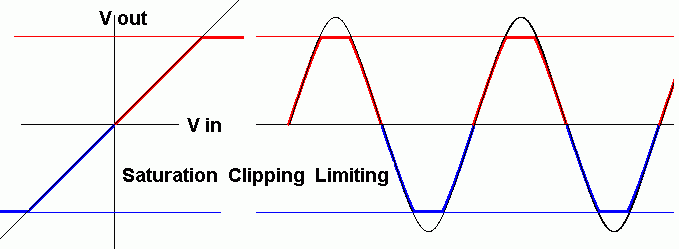
An opamp’s active region is defined by the voltage range the opamp can output without saturating. If for instance the positive supply voltage (VDD) is +15V and the negative supply voltage (VSS) is -15V, you might think that the active region is from -15V to +15V. The active region is always narrower than the supply voltage. You can get pretty close with so called rail-to-rail opamps, but you won’t be able reach those outer extremes.
Saturation occurs when the combination of a) input voltage and b) opamp configuration results in a theoretically output voltage outside of the active region.
Say for instance that you have a non-inverting amplifier with a gain of 10, an active region of -14V to +14V and 5V on the non-inverting input pin. Theoretically you should get 50V on the output pin, but it will instead saturate at 14V.
Maximum Ouput Voltage Swing
This brings us to the first parameter we’re going to look at: the maximum output voltage swing. This parameter specifies how close to VDD and VSS the output voltage can get. Microchip’s MPC6001, which we’ll use as an example opamp for the rest of this blog post, has a maximum ouput voltage swing of minimum VSS + 25mV and maximum VDD – 25mV, which defines the active region.
Current Limitation
In addition to the voltage limits of the output we also have a current limit. This limit is most commonly between 10mA and 100mA for general purpose opamps, but you do of course have exceptions which handle more or less than that.
Supply Voltage and Current
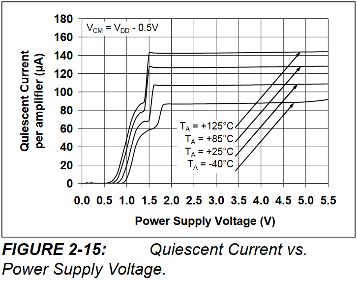
In addition to the obvious supply voltage range (1.8V – 6V on the MPC6001), you also have a less obvious idle supply current, often called quiescent current. This current is what the opamp draws from the power supply when it’s idle (no current and 0V on the output). On our MPC6001 this current is typically 100μA at 5VDD, but may vary a lot (as seen below).
Input
Let’s talk about input stuff.
Input Offset Voltage
Do you remember the golden rule #2 from part 1 which says that an opamp with feedback will set its output so that the inputs are at the same voltage level? This implies that if the inputs are equal, the opamp won’t do anything on its output pin, i.e. it will set it to zero volts.
In real life, however, what the opamp perceives as identical voltage on the input pins might not actually be identical in real life. This is called the input offset voltage. Common input offset voltage values can be between 1mV to 10mV and changes over temperature and time.
Input Current
Golden rule #1 says that no current flows in or out of the input pins. This is not 100% true. Opamps have something called input bias current which is the current at the input pins. This is usually really small (e.g. 1pA), but can increase quite drastically at higher temperatures as shown in the graphs below.
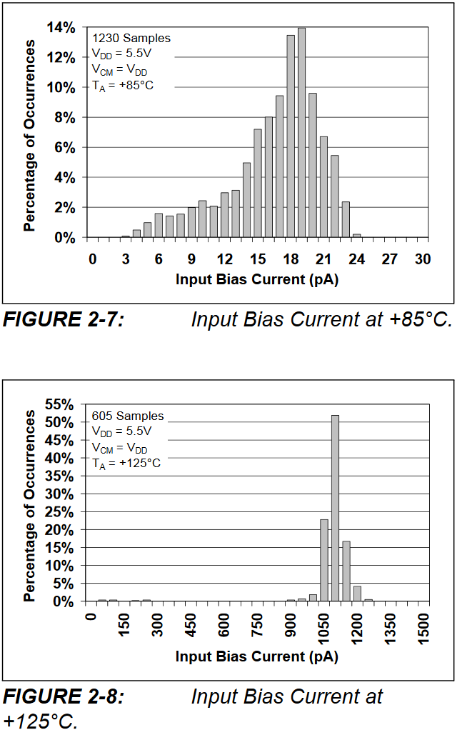
You also have input offset current which is the difference between the input currents, and is also very low (typically 1pA).
Common Mode Input Range
The input also has its own little “active region” called common mode input range (or common mode voltage range). This is defined relative to VDD and VSS and specifies what kind of input voltages you can apply before the opamp starts to act abnormally. On the MPC6001 the common mode input range is from VSS – 0.3V to VDD + 0.3V. Note that this range actually exceeds the power supply range.
Common Mode Rejection Ratio
You often want to keep differences between the input, but supress voltage fluctuations and noise which is common for both inputs. The common mode rejection ratio is a property that specifies the opamp’s ability to “remove” these unwanted common-mode signals. Ideally this would be infinitely high, but this is not possible in real life. We’re not going to go deeper into the definition of this parameter, except that it is specified in dB and that higher is better.
Frequency Response
How quickly an opamp can react to input changes is an important parameter.
Slew Rate
An ideal opamp can change output voltage infinitely fast. A non-ideal opamp cannot. Opamps have something called slew rate which says how fast they can change the voltage on the output pin. Slew rate is specified as V/s and varies between 0.1V/μs to several thousand V/μs. Similarly to the input current, the slew rate varies with temperature as well as supply voltage.
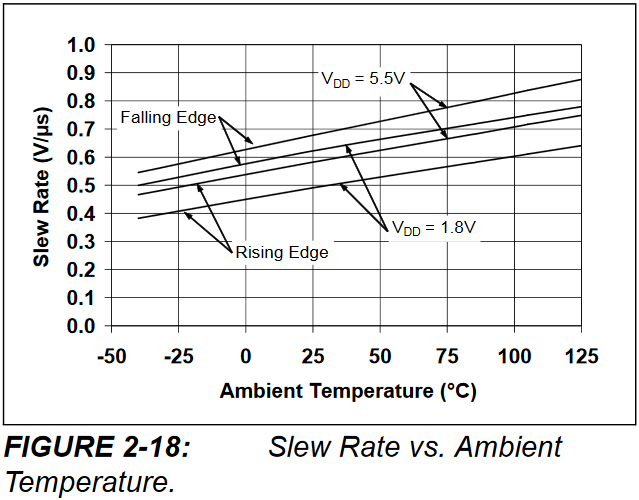
If you apply a signal with too high frequency for the opamp’s slew rate to follow, you’ll get what’s called slew-rate-induced distortion. Your opamp will get dazed and confused, and will output an undesired signal.
Gain Bandwidth Product
Another, and arguably more common way to specify the frequency response of an opamp is by using the gain bandwith product parameter. This is a bit more intricate to explain and understand. Let’s look at a graph first:
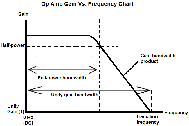
The gain bandwidth product is the result you get by multiplying the gain and the frequency at any given point between the full-power bandwidth and the unity-gain bandwidth. That’s where the line is straight after the bend in the graph above. The result will be the same no matter where on this line segment you choose to calculate this.
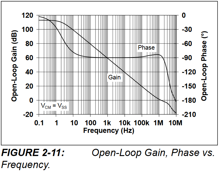
On our trusted MPC6001, the gain bandwidth product is 1MHz, as shown in the graph above. The higher this number is, the faster the opamp is.
Summary
The opamp is a complex component with a lot of different properties. Almost all of these properties depends on temperature, supply voltage, input common mode voltage and/or other parameters. Finding the right opamp for your application might be a challenge, since there are thousands of different opamps out there. We hope that this blog post can help you a bit with that decision now that we’ve explained some of the most important characteristics you’ll find in the datasheets.
We might continue with this series later, since there’s still a BUNCH of interesting opamp material yet to cover.